Engineering grain architecture in epitaxial aluminum on miscut substrates toward various clean limits and giant superconductivity modulation
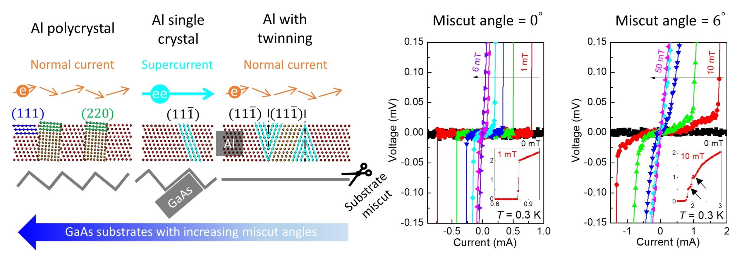
Aluminum (Al) has attracted considerable attention for uses in photonic, electronic, and quantum devices. Its grain architecture governs surface roughness, electron and light scattering, and quantum decoherence, all of which critically affect device performance. Enhancing crystalline domain size and refining granularity control remain an ongoing research focus for producing ultraclean nanofilms. This study investigates the crystallinity of epitaxial Al grown on miscut GaAs substrates and examines its influence on Al superconductivity. The introduction of a substrate miscut alters Al growth kinetics, enabling the formation of twinned grains, polycrystalline structures, and micrometer-scale single crystal. Variations in grain architecture result in significant modulation of the superconducting critical temperature, current, and magnetic field, respectively, while maintaining constant channel geometries. Reducing macroscopic grain boundaries decreases the Al nanofilm resistivity but enhances strain-induced crystallinity deterioration, driving a transition from type-I to type-II-like superconducting behavior. We suggest that preparing Al nanofilms, which approach an ultraclean limit in terms of surface quality, crystallinity, and transport properties, requires careful control of substrate miscut as well as the grain architecture. These findings highlight a tunable approach to controlling Al granularity and superconductivity via miscut, lattice-mismatched substrates.
On-chip quantum sensing of Kondo spins in a high-mobility quasi-one-dimensional nanoconstriction
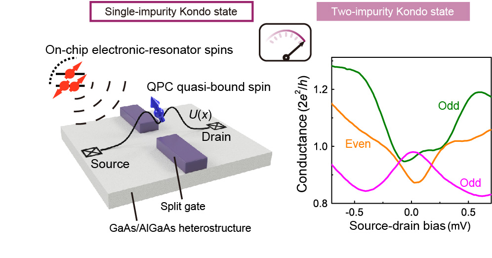
Not only quantum dot but also quantum point contact can bound electron spins to realize local and nonlocal Kondo spin entanglement! The precise nature of Kondo spins has remained enigmatic when extended to multiple spin impurities or, more intriguingly, when the localized spin itself may already be the consequence of many-body interactions in a presumably-delocalized open nanoconstriction, such as a quantum point contact (QPC). It is experimentally challenging to distinguish the Kondo state from other coexisting many-body spin states in such a strongly correlated system. Here we lithographically define an all-on-chip electronic resonator (ER) and a QPC in a high-mobility GaAs/AlGaAs heterostructure transistor. Local Kondo screening of the QPC spin and nonlocal spin singlet across the ER-QPC integration are controllable in response to ER occupancy parity. We also show that the 0.7 anomaly, another strongly-correlated state in QPCs, not only has a different physical origin but furthermore counteracts the Kondo spin singlet. These results demonstrate a noninvasive quantum method for sensing spontaneous magnetic impurities within an open nanoconstriction.
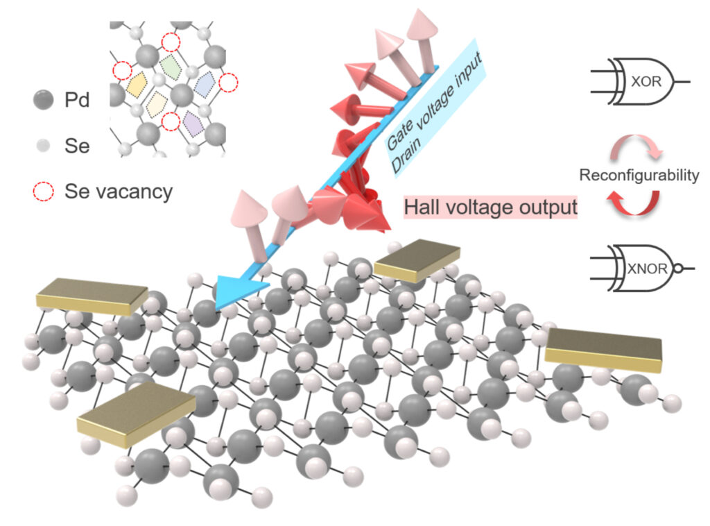
All-electric functional PdSe2 planar-Hall logic field-effect transistors
Advanced Functional Materials, 35, 2412896 (2025)
New computing architectures can be built not only on qubits but also on 2D crystals with gate-tunable band anisotropy! 2D semiconductor logic has advantages of reconfigurable multi-state operation through extrinsic charge-transfer doping mechanisms such as molecular adsorption and light illumination. However, their precise control remains challenging and they bring defects and blur the specified logic protocol for computation. Semiconducting 2D layered palladium diselenide (PdSe2), a noble transition-metal dichalcogenide with a puckered pentagonal atomic structure, has shown great potential for multi-functional devices owing to its low crystal symmetry. Here, anisotropic charge transport in band-like, variable-range hopping, and quantum-dot tunneling regimes are demonstrated in a multi-terminal PdSe2 transistor. The gate-tunable oscillatory Hall charge movement due to zero-magnetic-field pseudo-planar Hall effect provides a physical reference to encode the dynamical PdSe2 anisotropic energy dispersions up to room temperature. Complementary XOR and XNOR logic relations between Hall voltage output and gate/drain voltage inputs are identified and they are reconfigurable with each other by changing the current injection direction. Controlling the layer number further reconfigures the planar-Hall effect polarity and Hall logic. This work paves an all-electric reconfigurable way to a planar-Hall logic transistor, enabling the initialization, manipulation, and detection of anisotropic electronic states, and offers opportunities for next-generation computing utilizing multiple energy bands of engineered anisotropies in puckered pentagonal 2D materials.
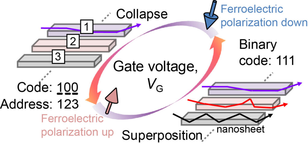
Quantum-inspired current superposition and collapse in gate-all-around and planar-gated silicon-based transistors
Advanced Materials 35, 2301206 (2023)
Inspired by the quantum collapse of superposition states for information decoding in quantum circuits, the implementation of analogous current path collapse to facilitate the detection of microscopic circuits by modifying their network topology is explored. Here, the superposition and collapse of current paths in gate-all-around polysilicon nanosheet arrays are demonstrated to enrich the computational resources within transistors by engineering the channel length and quantity. Switching the ferroelectric polarization of Hf0.5Zr0.5O2 gate dielectric, which drives these transistors out-of-equilibrium, decodes the output polymorphism through circuit topological modifications. Furthermore, a protocol for the single-electron readout of ferroelectric polarization is presented with tailoring the channel coherence. The introduction of lateral path superposition results into intriguing metal-to-insulator transitions due to transient behavior of ferroelectric switching. This ability to adjust the current networks within transistors and their interaction with ferroelectric polarization in polycrystalline nanostructures lays the groundwork for generating diverse current characteristics as potential physical databases for optimization-based computing. (LinkedIn)
Control of coherent spin dynamics via superposition of spin-orbit-induced magnetic fields

Nature Communications 8, 15997 (2017)
We demonstrate that the spatial spin splitting of a coherent beam of electrons can be achieved and controlled using the interplay between an external magnetic field and Rashba spin–orbit interaction in semiconductor nanostructures. The technique of transverse magnetic focusing is used to detect this spin separation. More notably, our ability to engineer the spin–orbit interactions enables us to simultaneously manipulate and probe the coherent spin dynamics of both spin species and hence their correlation, which could open a route towards spintronics and spin-based quantum information processing.
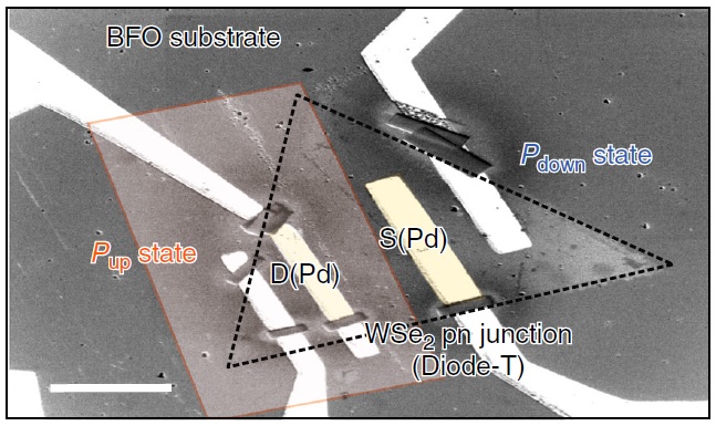
Semiconducting pn diode from interplay of semiconducting WSe2 and ferroelectric BiFeO3
Nature Communications 9, 3143 (2018)
By utilizing a locally reversed ferroelectric polarization, we laterally manipulate the carrier density and created a WSe2 pn homojunction on the supporting ferroelectric BiFeO3 substrate. This non-volatile WSe2 pn homojunction is demonstrated with optical and scanning probe methods and scanning photoelectron microspectroscopy. A homo-interface is a direct manifestation of our WSe2 pn diode, which can be quantitatively understood as a clear rectifying behavior. The non-volatile confinement of carriers and associated gate-free pn homojunction can be an addition to the 2D electron–photon toolbox and pave the way to develop laterally 2D electronics and photonics.
Superconducting diode from interplay of GaAs-based 2DEG and aluminum superconducting nanofilm

Scientific Reports 3, 2274 (2013)
We have studied a hybrid nanoelectronic system which consists of an GaAs/AlGaAs two-dimensional electron gas (2DEG) in close proximity (∼ 70 nm) to an Al superconducting nanofilm. By tuning the current through the Al film, we can change the conductance of the 2DEG and furthermore vary the effective disorder in the Al superconducting film in a controllable way. When a high current is injected into the film, screening which couples the Al film and the 2DEG results in a collapse of anti-symmetric behavior in the current-voltage characteristics, V(I) ∼ –V(-I), which holds true in a conventional superconductor. Our results may open a new avenue of experimentally realizing a superconducting diode.